Some estimates indicate double-digit market growth in 2024, largely driven by AI technology and trends. 1 Given the substantial time and financial investments required to ramp up semiconductor production 2, improving yield and decreasing losses is one of the best ways to keep up with the increasing demand and prevent supply shortages.
Few industries place a greater emphasis on cleanliness than the semiconductor sector. Microchips and electronic components are very delicate and require production in a controlled environment using materials and equipment that meet the strictest cleanliness standards. The semiconductor manufacturing process involves a complex sequence of processes and steps, during which strict cleanliness requirements must be met to guarantee consistent quality and yield of the product. Each step of its production, testing, packaging, and transportation presents a risk of contamination.3 This also means that all equipment used for its production, from large machinery to small components, must be produced, packed, and transported in adherence to the same rigorous cleanliness standards.
Cleanroom-compliant packaging plays a crucial role in this process by protecting manufacturing equipment and components against contamination, which can lead to defective devices, yield losses, and compromised performance. 4 Therefore, it is crucial to ensure consistent quality and safety from the start. This can be achieved by using custom-designed cleanroom-compatible packaging that is manufactured, cleaned, assembled, and packed in accordance with stringent international requirements. But what exactly is cleanroom-compatible packaging, and how do they help ensure uninterrupted semiconductor supply?
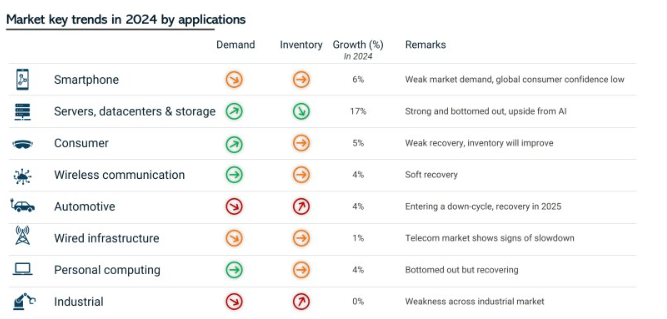
The AI technology is the driving force behind the semiconductor growth in 2024. Source: EE Times5 after Strategic Semiconductors6
Contamination Control Increases the Yield
Cleanrooms are an integral part of the semiconductor manufacturing process. Their adherence to stringent air quality requirements dictates their classification, a system established by the International Organization for Standardization (ISO). This classification is based on the concentration of particles present in each cubic meter of air.7 ISO 5 to ISO 7 cleanrooms are common requirements for packaging in the semiconductor manufacturing industry because they are highly effective at protecting products from contamination. Particulate matter, static electricity, humidity, and outgassing pose significant threats at the production and packaging sites, emphasizing the critical role cleanrooms play in maintaining the integrity of the process.
Cleanrooms offer several benefits for the semiconductor manufacturing process. By preventing contamination, they enhance production yield and reduce product flaws, resulting in higher quality goods and optimal functionality. 8 This not only saves costs that would otherwise be used to cover damages but also preserves the company's reputation. In summary, cleanrooms are essential environments crucial for preserving the quality of semiconductor products, manufacturing equipment, and components, and for streamlining production processes to achieve maximum effectiveness.
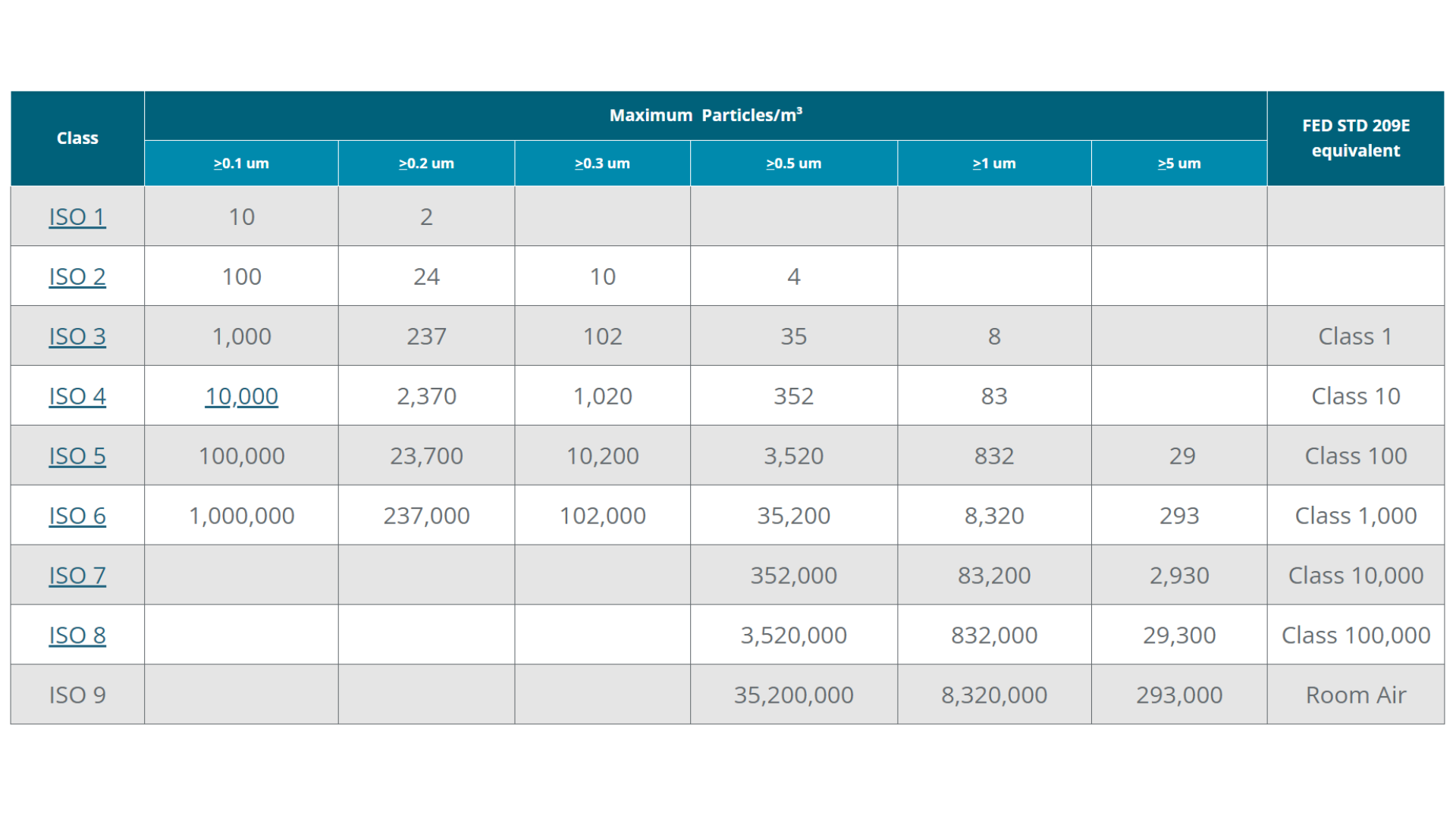
Cleanrooms, classified by particle concentration per cubic meter, are crucial for protecting semiconductor products from contamination. Source: American Cleanroom Systems
Enhanced Safety And Sustainability
Designing inherently cleanroom-compliant packaging is crucial. As there is no one-size-fits-all solution, packaging design and development should be customized to fit various equipment and components, from dicing tools to probing machines. All that to ensure not only safety but also environmental savings. Expendable cleanroom packaging solutions are a good example here, as they were designed in a way that effectively minimizes material usage and optimizes the supply chain. By reducing the space and weight of transported goods, they lower transportation costs and save CO2-eq emissions. Cleanroom-compliant thermoformed packaging solutions are another good example. Not only is their smooth surface easier to clean than PE foam, but also their special ESD properties block electrostatic discharge, reducing product defects and particle attraction to its surface. Additionally, thermoformed trays significantly reduce particle shedding compared to PE foams. Thermoformed packaging is often made from 100% recycled thermoformed material, which not only saves resources but also has significantly lower post-production outgassing.
Returnable, cleanroom-approved packaging solutions enhance efficiency and visibility across the circular flows but also play a significant role in reducing environmental impact. These solutions operate in a closed-loop system, meaning they can be easily repaired and reused, thereby minimizing the resource waste associated with single-use packaging. Incorporating advanced sensors means that critical environmental data such as shock, temperature, and humidity can be continuously monitored in real-time. This capability ensures the integrity of your shipments, helping to maintain product quality and reduce waste while also promoting sustainability within the supply chain.

Returnable, cleanroom to cleanroom approved packaging solutions enhance efficiency and visibility and significantly reduce environmental impact.
Global Quality Assurance
Maintaining cleanliness is paramount throughout the semiconductor production process to ensure top-notch quality, yield, and performance. This intricate task demands meticulous attention to detail, strict adherence to protocols, and seamless collaboration across the entire supply chain. Semiconductor manufacturing is one of the most complex and globally interconnected industrial supply chains worldwide. This means that the quality of work performed in cleanrooms should be preserved, regardless of the geography.
At Nefab, we bring extensive expertise in designing, manufacturing, and cleaning cleanroom-compliant packaging solutions, as well as in cleaning and packing our customers’ products. From custom steel assemblies and plastic pallets to flight cases and cleanroom bags and sheets, we cater to diverse needs in the semiconductor industry. Moreover, we excel in developing, implementing, refurbishing, cleaning, and managing returnable, modular solutions. These solutions ensure safe transportation of products between cleanrooms, underscoring our commitment as a global player in facilitating seamless semiconductor manufacturing processes.