- 新聞與見解
- 2024
- The Role of Data and Circular Packaging Solutions in Reducing Semiconductor Industry Scope 3 Emissions
The Role of Data and Circular Packaging Solutions in Reducing Semiconductor Industry Scope 3 Emissions
Tackling the challenge of decarbonizing the semiconductor industry is no small feat. A crucial first step is for companies to accurately assess their current greenhouse gas (GHG) emissions. With this insight, they can implement meaningful changes, such as automating workflows, reducing waste, and adopting sustainable packaging solutions.
Semiconductors are at the heart of modern technology, powering everything from the smartphones in our pockets to the cars on our roads. As the world becomes increasingly digital, the demand for chips is skyrocketing, driven by breakthroughs in processing power and cutting-edge innovations. Since 1965, semiconductors have advanced at an incredible pace, following Moore's Law, which predicts the doubling of transistors on a chip every two years 1. This rapid progress has made it possible to create compact devices with vast computational power. But with this growth comes a pressing responsibility: the semiconductor industry must find ways to reduce its emissions in line with the 2015 Paris Agreement 2.
Tackling the challenge of decarbonizing the semiconductor industry is no small feat. A recent BCG3 report highlights just how difficult the road ahead is, especially for companies striving to meet the 1.5°C climate goal. It’s not simply a matter of improving production efficiency — every part of the value chain must contribute, including often-overlooked areas like packaging and logistics. A crucial first step is for companies to accurately assess their current greenhouse gas (GHG) emissions. With this insight, they can implement meaningful changes, such as automating workflows, reducing waste, and adopting sustainable packaging solutions. These actions play an important role in helping reduce emissions and moving the semiconductor industry toward a more sustainable future.
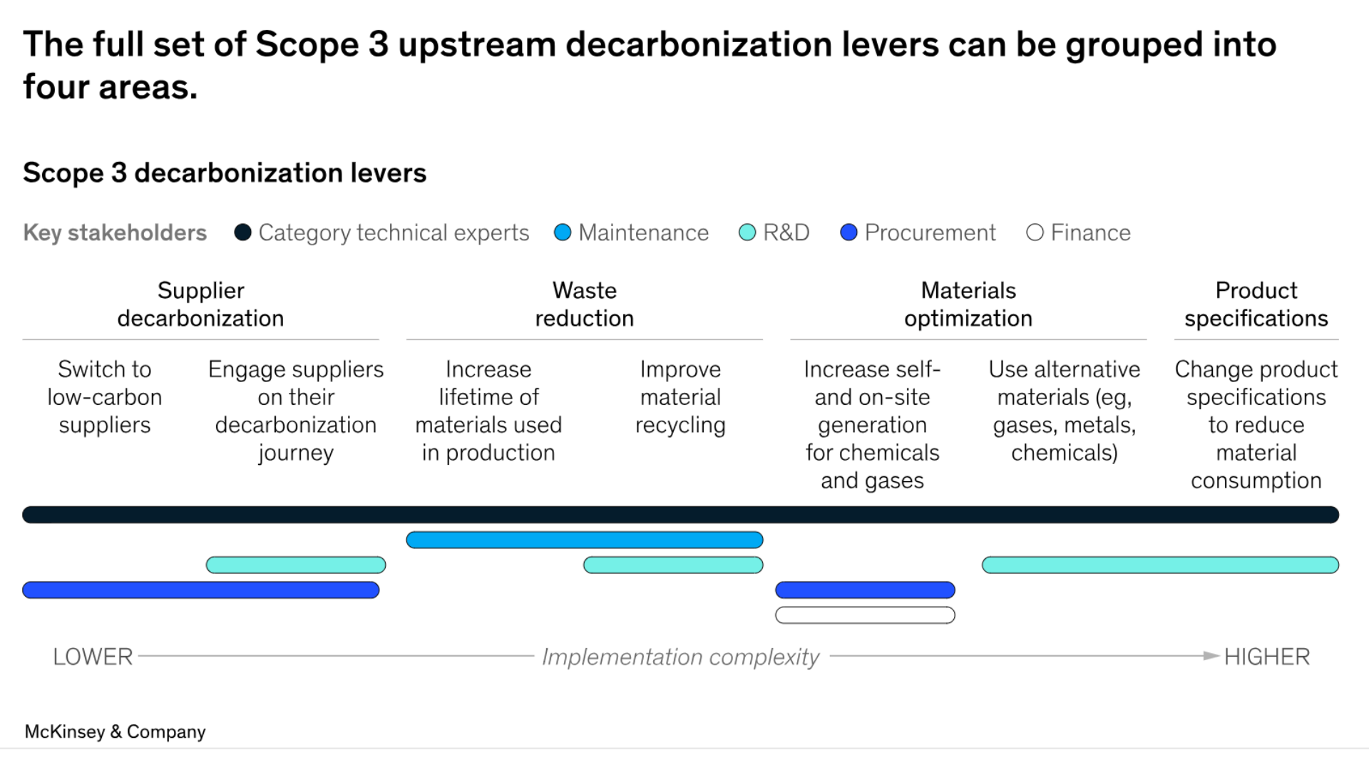
Extending the lifespan of production materials and enhancing material recycling are key strategies for semiconductor companies to minimize waste and reduce Scope 3 emissions. Source: McKinsey & Company
The Power of Data
It's no surprise that many refer to the 21st century as the "century of data." Data has become a driving force in today’s world, playing a crucial role in helping us make better decisions, increase efficiency, and foster innovation across various sectors of the economy. According to recent findings, a significant 68% of CEOs are gearing up for substantial investments in data and technology within the next year 4. Data plays a crucial role in helping organizations achieve their net zero targets by enhancing visibility into baseline emissions levels and identifying emissions hotspots. A significant challenge is that many organizations overlook Scope 3 emissions (on average, 1 in 5 organizations measure scope 3 emissions), which can account for 65‒95% of a company’s carbon footprint 5. According to the same study, while 85% of organizations recognize the value of emissions measurement and analytics, many struggle to effectively capture and utilize this data. This underscores the urgent need to strengthen data management capabilities to successfully transition to net zero.
GreenCalc™ collects comprehensive data on emissions, waste, returnability, and material types, allowing companies to optimize their sustainable packaging strategies.
GreenCalc™ is a powerful, data-driven Life Cycle Analysis (LCAs) tool designed to evaluate packaging and logistics flows, enabling organizations to make informed decisions as they strive for net zero. By focusing on sustainable packaging design, it addresses the limitations of current linear flows, encouraging the development of packaging solutions that enhance resource utilization through reusability and recyclability. GreenCalc™ collects comprehensive data on emissions, waste, returnability, and material types, allowing companies to optimize their sustainable packaging strategies. Furthermore, the Scope 3 GAIA dashboard provides customers with a clear environmental impact baseline, enabling them to monitor the effectiveness of their improvement initiatives and ensure consistent progress toward their sustainability objectives.
Scope 3 emissions often go unmeasured but can make up a large portion of an organization’s carbon footprint. Conducting Life Cycle Analysis (LCAs) is essential to mitigating these emissions through sustainable design strategies, such as selecting low-carbon packaging materials and optimizing product designs. Source: Capgemini Research Institute
Circular Innovation
In the semiconductor industry, adopting innovative and eco-friendly packaging solutions has become essential for reducing emissions and minimizing waste. One exciting development is the rise of thermoformed plastic packaging, specifically designed for returnable flows. These trays help decrease reliance on one-way packaging, which is a major contributor to waste in the supply chain. Crafted from 100% recycled post-consumer HDPE, they reduce the need for virgin materials, making a positive impact on the environment. When these trays reach the end of their lifecycle, they are not just tossed aside; they are collected, cleaned, and the material is extruded to create new recycled trays. This keeps the plastic in circulation and plays a significant role in lowering CO2-eq emissions while also cutting costs—truly a win-win for both the environment and businesses.
Thermoformed trays are also designed for performance, especially when it comes to protecting sensitive semiconductor equipment and components.
But the benefits don’t stop there. Thermoformed trays are also designed for performance, especially when it comes to protecting sensitive semiconductor equipment and components. They offer much cleaner particle performance than standard foams, ensuring that delicate parts remain uncontaminated during storage and transport. One of their standout features is their impressive nestability, which can save up to 85% of space during inbound transport and storage. This space-saving efficiency not only reduces logistical costs but also translates into significant cuts in CO2-eq emissions. By embracing these circular packaging solutions, companies are not just enhancing their operations; they’re also making meaningful strides toward a more sustainable future in the semiconductor industry.

Thermoformed trays are designed to be nestable, significantly reducing space in logistical flows compared to traditional PE foam packaging. Source: Nefab
Paving the Way for the Better Future
The path to a net-zero semiconductor industry is challenging but achievable through a combination of data-driven strategies and innovative, circular packaging solutions. By leveraging tools like GreenCalc™ to measure and manage Scope 3 emissions and embracing circular materials like thermoformed trays, companies can significantly reduce their environmental impact. As the demand for semiconductors continues to grow, the industry's commitment to sustainability will be crucial in driving an environmentally conscious future.
為了更美好的明天,我們在供應鏈中節約資源。
想瞭解更多資訊?
聯繫我們
Contact us to learn more about our smart and sustainable solutions.
瞭解更多資訊
Solutions for the Semiconductor Industry
Engineered for Precision and Sustainability
GreenCalc
Nefab’s own certified calculator measures and quantifies financial and environmental savings in our solutions
Global Engineering Network
250 engineering experts in more than 30 locations